


Optimizing the electrical performance of solution-processed polymer and small molecule electronic devices
The changes in the optoelectronic properties of organic thin films can be dramatic even if the underlying structural and morphological changes that induce them are small. . This is due to the steric, spatial, and angular complexity and inner structure of many organic molecules, resulting in a highly complex relationship between molecular geometry, supramolecular assembly, and the resulting film morphology and charge transport. The introduction of the solvent in solution-processing further complicates matters since it couples the film fabrication process to many parameters such as coating speed, solvent choice, temperature, concentration in addition to the surface energetics of the substrate.
However, though this makes it challenging to optimize and balance these many influences, controlled solution processing also leads to potentially high-throughput, large-area fabrication of low-cost electronics, and in fact also represents a powerful tuning knob for morphology, texture and even molecular packing: for example, solution processing can achieve molecular packing motifs and stabilize polymorphs of a material that cannot be fabricated by vapor-phase processing.
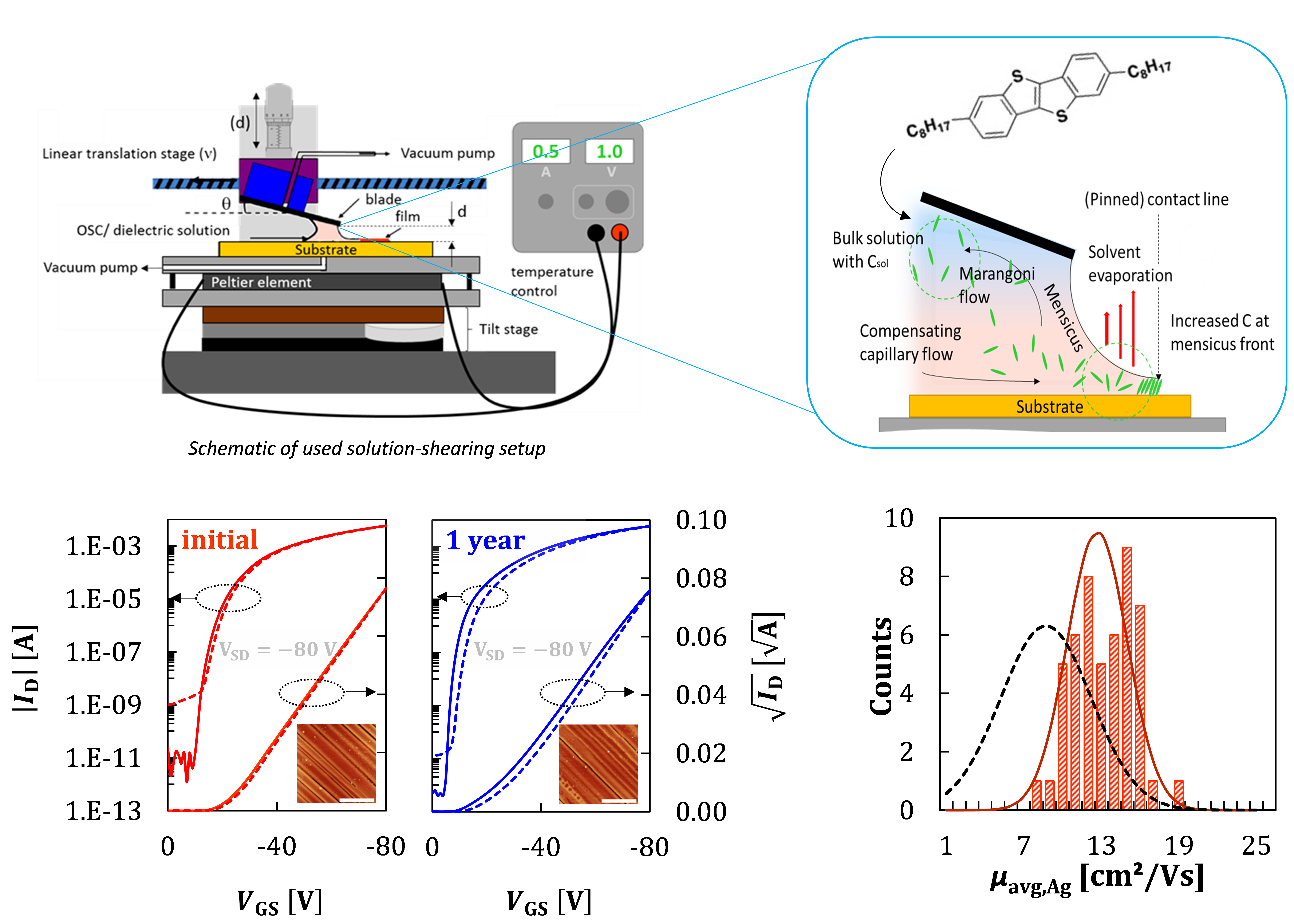
Following the discoveries we initially made with the material TIPS-pentacene – that the blade coating method we call “solution shearing” is capable of producing very high performance thin films and OFET devices, and can stabilize even what in the bulk is an exclusively high-temperature polymorph[1,2] – we employ solution shearing for a wide array of device-related materials. We sometimes spin-coat, but most often “shear-coat” (see Image) small molecule semiconductors [2–5], semiconducting polymers[6–9], conducting polymers[10], insulating polymers[11], blends of insulating polymers and small molecule semiconductors[3,4], and lately also metal oxide semiconductors and dielectric layers for conventional OFETs transistors[11] or vertical transistor devices[5]. The goal in these works is to produce thin films of high quality that show state-of-the-art performance or allow us to produce and test novel device architectures.
While our “solution shearing” coaters are clearly lab-scale tools that only emulate important properties of larger, industrial-grade coating tools, they allow us to study the effect of the coating conditions and physics in a flexible manner. It is a test-bed to study modifications from piezo crystal-introduced vibrations[7] of the coating blade to roll-to-roll setups that allow as to monitor film growth in-situ[12].
- Y. Diao, L. Shaw, Z. Bao, S. C. B. B. Mannsfeld, Energy Environ. Sci. 2014, 7, 2145.
- Y. Diao, K. M. Lenn, W.-Y. Y. Lee, M. A. Blood-Forsythe, J. Xu, Y. Mao, Y. Kim, J. A. Reinspach, S. Park, A. Aspuru-Guzik, G. Xue, P. Clancy, Z. Bao, S. C. B. B. Mannsfeld, J. Am. Chem. Soc. 2014, 136, 17046.
- K. Haase, C. Teixeira da Rocha, C. Hauenstein, Y. Zheng, M. Hambsch, S. C. B. Mannsfeld, Adv. Electron. Mater. 2018, 4, 1800076.
- C. Teixeira da Rocha, K. Haase, Y. Zheng, M. Löffler, M. Hambsch, S. C. B. Mannsfeld, Adv. Electron. Mater. 2018, 4, 1800141.
- D. Kneppe, F. Talnack, B. K. Boroujeni, C. Teixeira da Rocha, M. Höppner, A. Tahn, S. C. B. Mannsfeld, F. Ellinger, K. Leo, H. Kleemann, Mater. Today Energy 2021, 21, 100697.
- M. Hambsch, T. Erdmann, A. R. Chew, S. Bernstorff, A. Salleo, A. Kiriy, B. Voit, S. C. B. Mannsfeld, J. Mater. Chem. C 2019, 7, 3665.
- C. Teixeira da Rocha, G. G. Qu, X. Yang, R. Shivhare, M. Hambsch, Y. Diao, S. C. B. S. C. B. Mannsfeld, ACS Appl. Mater. Interfaces 2019, 11, 30079.
- K. Ditte, J. Perez, S. Chae, M. Hambsch, M. Al-Hussein, H. Komber, P. Formanek, S. C. B. Mannsfeld, A. Fery, A. Kiriy, F. Lissel, Adv. Mater. 2021, 33, 2005416.
- K. Ditte, N. Kiriy, J. Perez, M. Hambsch, S. C. B. Mannsfeld, Y. Krupskaya, R. Maragani, B. Voit, F. Lissel, Polymers (Basel). 2021, 13, 1435.
- B. J. Worfolk, S. C. Andrews, S. Park, J. Reinspach, N. Liu, M. F. Toney, S. C. B. Mannsfeld, Z. Bao, Proc. Natl. Acad. Sci. 2015, 112, 14138.
- K. Haase, J. Zessin, K. Zoumboulis, M. Müller, M. Hambsch, S. C. B. Mannsfeld, Adv. Electron. Mater. 2019, 5, 1900067.
- X. Gu, Y. Zhou, K. Gu, T. Kurosawa, Y. Guo, Y. Li, H. Lin, B. C. Schroeder, H. Yan, F. Molina-Lopez, C. J. Tassone, C. Wang, S. C. B. Mannsfeld, H. Yan, D. Zhao, M. F. Toney, Z. Bao, Adv. Energy Mater. 2017, 7, 1602742.
Novel organic device types for non-volatile memory and artificial synapse applications
Although memories represent by far the largest part of conventional (silicon-based) electronic systems, work on organic memories is severely lagging behind the research efforts regarding organic field-effect transistors (OFETs). Although a lot of the existing organic memory concepts are entirely electronic in nature (i.e., they are both written to and read from by electrical means), some application would tremendously benefit from the ability to read and write optically in addition to the purely electrical way of achieving read/write functionality – for example contactless applications similar to “barcode”-scanners that require read and write without direct physical contact or optical sensors that “remember” light exposure.
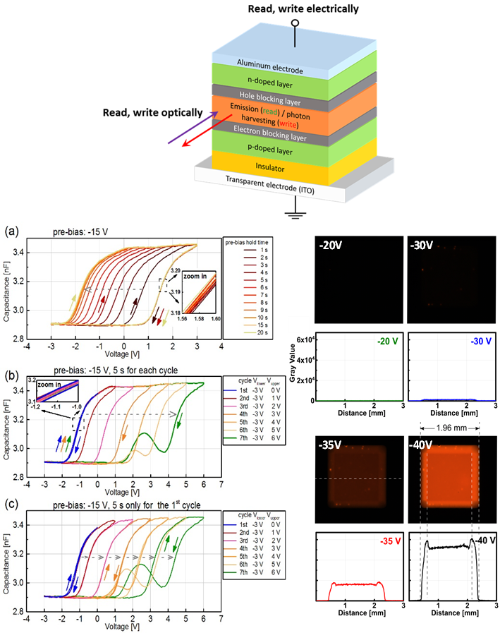 |
We recently were able to observe a distinct memory window and electrical reading and writing of memory states in OLED structures that contain an additional capacitive element.[1] Due to the fact that the device contains a p-i-n junction, one of the memory states can already also be detected by visible light emission. These results are highly promising – not only due to the simplicity of the device compared to FLASH-type floating gate device structures[2,3] but also due to strong indications for a multibit storage capability and the photonic access to the memory states. We are currently developing this memory to be accessible both fully electrically and independently fully optically, but also explore their uses as memcapacitive elements in neuromorphic organic circuits. |
- Y. Zheng, A. Fischer, M. Sawatzki, D. H. Doan, M. Liero, A. Glitzky, S. Reineke, S. C. B. Mannsfeld, Adv. Funct. Mater. 2019, 1907119, 1907119.
- Kaltenbrunner, P. Stadler, R. Schwödiauer, A. W. Hassel, N. S. Sariciftci, S. Bauer, Adv. Mater. 2011, 23, 4892.
- S. Lee, H. Seong, S. G. Im, H. Moon, S. Yoo, Nat. Commun. 2017, 8, 725.
Doping of organic semiconductors
The doping of organic semiconductors (OSCs) is, similar as for inorganic semiconductors, of great relevance for the realization of electronic devices. Possible functions of dopants are increasing the conductivity of a material, improving the injection or extraction of charge carriers at metal/semiconductor interfaces and the potential realization of p/n junctions. In contrast to inorganic semiconductors, like silicon, where doping is achieved by introducing foreign atoms into the crystal lattice, for OSCs usually molecules are used as dopants. The reason for this is that, unlike inorganic doped materials, the dopants in organic materials are not usually covalently linked to the host material which would cause diffusion of atomic dopants within the film or even diffusion out of the film. Instead, the addition of the larger dopant molecules produces stable films and leads to either an oxidation or reduction of the organic semiconductor, resulting in the generation of free charge carriers.
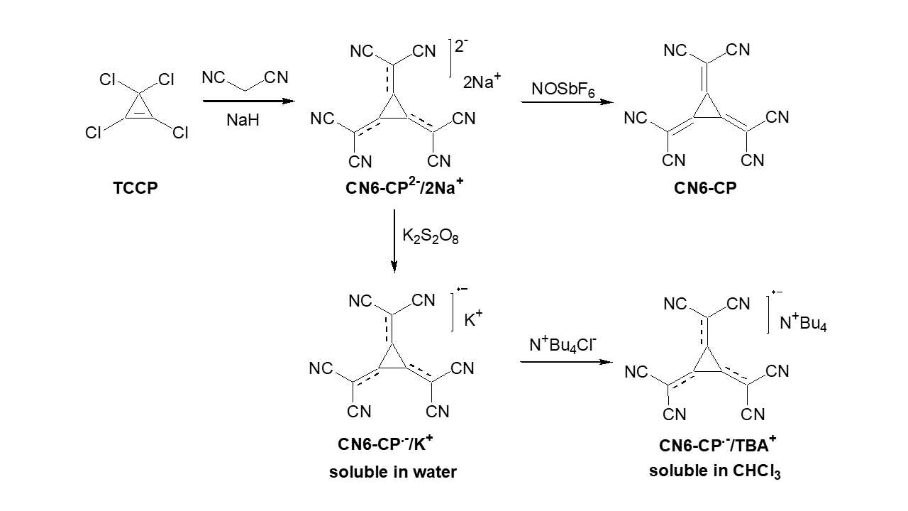
In recent years, we have studied, in close collaboration with the Leibniz Institute for Polymer Research (IPF), novel dopant molecules and their compatibility with a variety of OSCs.[1–5] One class of novel dopants is based on a hexacyano-substituted [3]-radialene. The neutral form of this molecule (CN6-CP) has shown to be a very strong dopant with donor-acceptor copolymers, unfortunately its poor solubility in organic solvents limits possible applications.[1] The solubility limitation can be solved by using the anion-radical of CN6-CP, which dependent on the used cation can be dissolved in water and a wide range of organic solvents. Although the reduction of CN6-CP leads to a lower doping strength it is still able to act as a dopant for a variety of p-type semiconductors, like P3HT.[2,3,5]
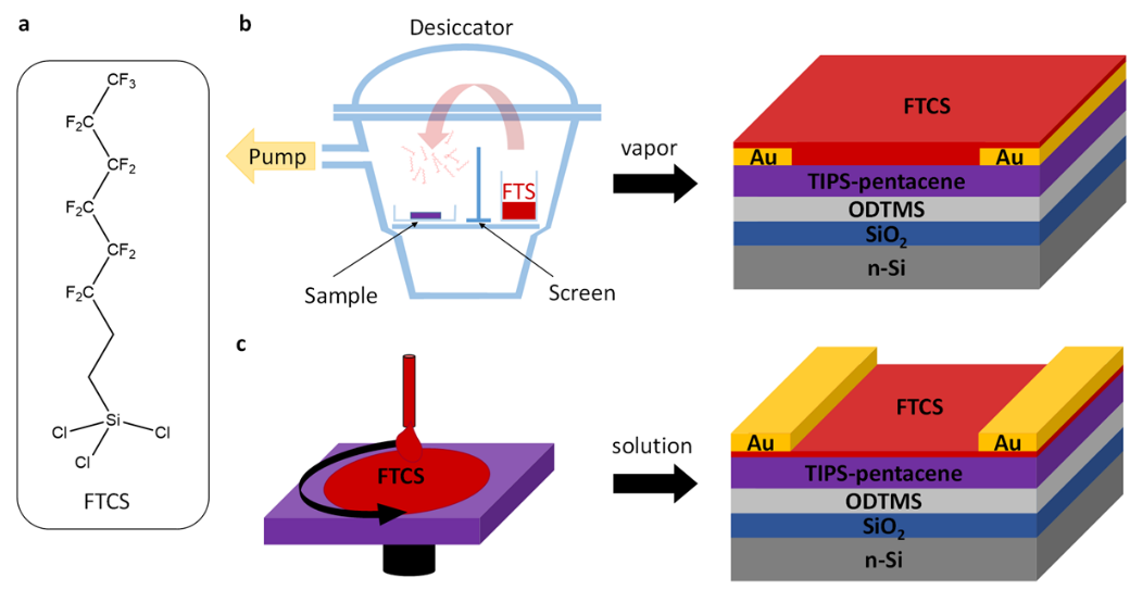
Besides studying novel dopant molecules, the processing of them as part of electronic devices is also of great interest. The most common approach is the blending of dopant and semiconductor in solution before processing the film by spin coating or other coating techniques. The downside of this fairly simple fabrication process that the presence of the dopant molecules in the bulk of the semiconductor can lead to changes in the structural order of the semiconductor or at least to the fact that they can act as traps or scattering centers for charge carriers. In our work we therefore focus on the sequential deposition of the dopant either from the gas phase or from solution. We have shown that this surface doping approach can be applied to both p-type[3,5–7] and n-type[8] semiconductors and can lead to improved conductivity, threshold voltage and/or charge carrier mobility. Alternatively, the dopant can be localized at the interface between semiconductor and dielectric in organic field-effect transistors to modify the threshold voltage and to a certain extent increase the charge carrier mobility of the device.[9] Here, we were not only able to show that by the use of self-assembled monolayers with amino groups the performance of n-type transistors can be tuned but also showed that the protonation of the amino group is a requirement for creating a free charge carrier in the semiconductor.
- Y. Karpov, T. Erdmann, I. Raguzin, M. Al-Hussein, M. Binner, U. Lappan, M. Stamm, K. L. Gerasimov, T. Beryozkina, V. Bakulev, D. V. Anokhin, D. A. Ivanov, F. Günther, S. Gemming, G. Seifert, B. Voit, R. Di Pietro, A. Kiriy, Adv. Mater. 2016, 28, 6003.
- Y. Karpov, N. Kiriy, M. Al-Hussein, M. Hambsch, T. Beryozkina, V. Bakulev, S. C. B. Mannsfeld, B. Voit, A. Kiriy, Chem. Commun. 2018, 54, 307.
- Y. Karpov, N. Kiriy, P. Formanek, J. Zessin, M. Hambsch, S. C. B. Mannsfeld, F. Lissel, T. Beryozkina, V. Bakulev, B. Voit, A. Kiriy, ACS Appl. Mater. Interfaces 2019, 11, 4159.
- Y. Karpov, T. Erdmann, M. Stamm, U. Lappan, O. Guskova, M. Malanin, I. Raguzin, T. Beryozkina, V. Bakulev, F. Günther, S. Gemming, G. Seifert, M. Hambsch, S. Mannsfeld, B. Voit, A. Kiriy, Macromolecules 2017, 50, 914.
- Y. Karpov, N. Kiriy, P. Formanek, C. Hoffmann, T. Beryozkina, M. Hambsch, M. Al‐Hussein, S. C. B. Mannsfeld, B. Büchner, B. Debnath, M. Bretschneider, Y. Krupskaya, F. Lissel, A. Kiriy, Adv. Electron. Mater. 2020, 6, 1901346.
- J. Zessin, Z. Xu, N. Shin, M. Hambsch, S. C. B. Mannsfeld, ACS Appl. Mater. Interfaces 2019, 11, 2177.
- J. J. Kim, S. Bachevillier, D. L. G. Arellano, B. P. Cherniawski, E. K. Burnett, N. Stingelin, C. Ayela, Ö. Usluer, S. C. B. Mannsfeld, G. Wantz, A. L. Briseno, ACS Appl. Mater. Interfaces 2018, 10, 26745.
- N. Shin, J. Zessin, M. H. Lee, M. Hambsch, S. C. B. Mannsfeld, Adv. Funct. Mater. 2018, 28, 1802265.
- N. Shin, K. S. Schellhammer, M. H. Lee, J. Zessin, M. Hambsch, A. Salleo, F. Ortmann, S. C. B. Mannsfeld, Adv. Mater. Interfaces 2021, 8, 2100320.
Understanding the structure-property relationship in organic solar cells
Organic solar cells established themselves as an alternative photovoltaic technology besides inorganic and hybrid solar cells and currently have reached power conversion efficiencies of up to 19%. One of the factors that paved the way to these improved efficiencies is the better understanding of the relationship between the chemical structure of the semiconductors, the microstructure of the fabricated films and the optoelectronic processes occurring in the films.
In our group, one focus is on polymer donor materials based on diketopyrrolopyrrole (DPP),[1–4] which is a very versatile polymer semiconductor used in a variety of devices. We investigated the influence the shape of the solubilizing side chain has on the film structure and showed that the position of the branching point in the alkyl chain has a strong influence on the crystallinity and the dimensions of the polymers in the films. These changes to the film morphology have significant implications on the optoelectronic properties of the solar cells. The higher degree of crystallinity by moving the branching point further away from polymer chain results in better charge transport properties leading to improved fill factors in the devices. Additionally, this change led to polymer fibers with larger diameter leading to enhanced recombination and therefore a reduction in generated photocurrent.[1] This together with our other studies on the effect of polymer molecular weight and processing conditions, like applied processing technique and used solvents, shows how complex the interactions between all these factors are and that all of them need to be considered when fabricating organic solar cells.[3,4]
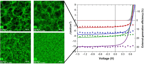
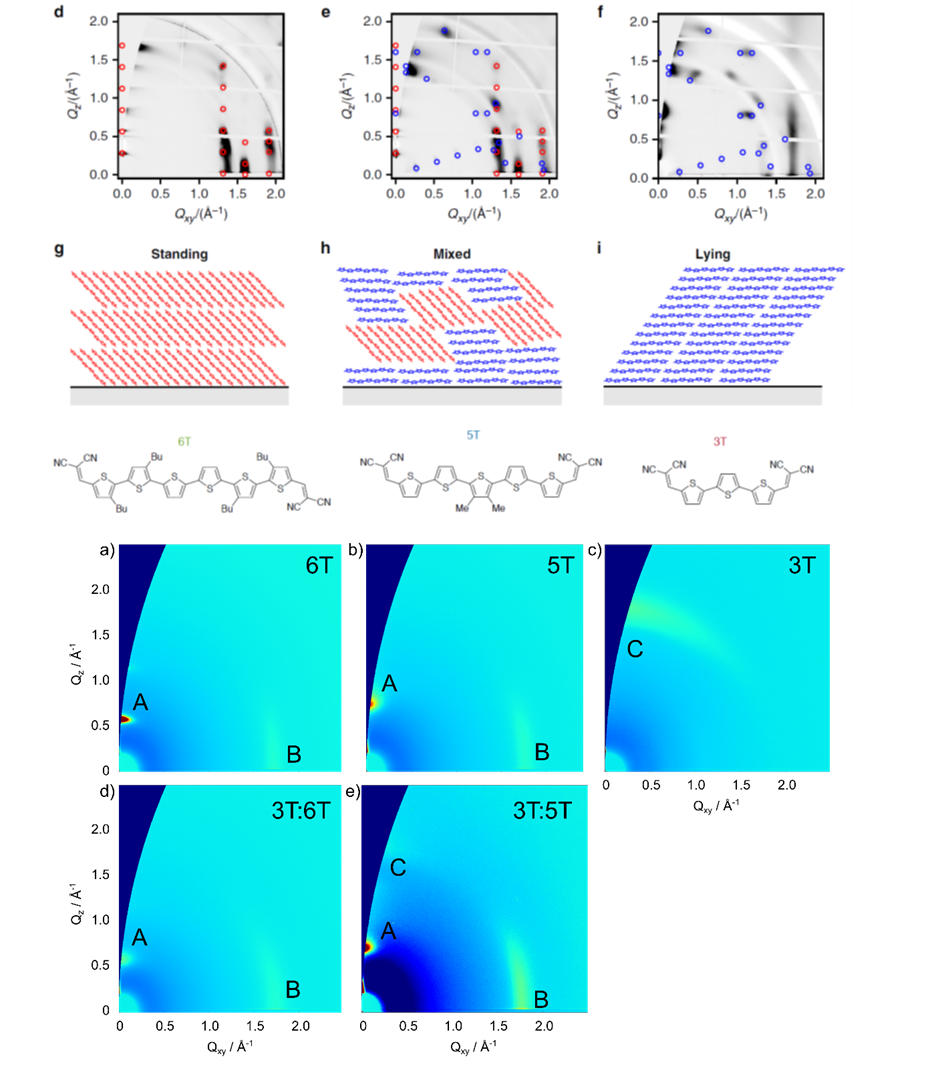
Similarly to the solution processed polymer:fullerene solar cells we also performed structural investigations on solar cells with vacuum deposited small molecules. By employing GIWAXS measurements, we were able to explain the changes in performance of homojunction solar cells using a thiophene-based semiconductor, when using various deposition conditions, by the orientation of the molecules in respect to the substrate (see top panel on the left). The relation between standing and lying molecules in these polycrystalline films defines the rate of charge separation leading to devices with improved conversion efficiency.[5] In a similar vein, we investigated how the blending of oligothiophenes with different numbers of thiophene rings can affect the structure of vacuum-deposited films leading to variations in the energy gap of the semiconductor film (see bottom panel on the left). This effect, similar to inorganic semiconductors allows the tuning of the band gap of organic semiconductors, something that so far has only been possible by changing the molecular structure of the semiconductors themselves.[6]
- R. Shivhare, T. Erdmann, U. Hörmann, E. Collado-Fregoso, S. Zeiske, J. Benduhn, S. Ullbrich, R. Hübner, M. Hambsch, A. Kiriy, B. Voit, D. Neher, K. Vandewal, S. C. B. Mannsfeld, Chem. Mater. 2018, 30, 6801.
- Shivhare, G. J. Moore, A. Hofacker, S. Hutsch, Y. Zhong, M. Hambsch, T. Erdmann, A. Kiriy, S. C. B. Mannsfeld, F. Ortmann, N. Banerji, Adv. Mater. 2021, 2101784, 2101784.
- A. Armin, P. Wolfer, P. E. Shaw, M. Hambsch, F. Maasoumi, M. Ullah, E. Gann, C. R. McNeill, J. Li, Z. Shi, P. L. Burn, P. Meredith, J. Mater. Chem. C 2015, 3, 10799.
- A. Armin, M. Hambsch, P. Wolfer, H. Jin, J. Li, Z. Shi, P. L. Burn, P. Meredith, Adv. Energy Mater. 2015, 5, 1401221.
- Dong, V. C. Nikolis, F. Talnack, Y.-C. Chin, J. Benduhn, G. Londi, J. Kublitski, X. Zheng, S. C. B. Mannsfeld, D. Spoltore, L. Muccioli, J. Li, X. Blase, D. Beljonne, J.-S. Kim, A. A. Bakulin, G. D’Avino, J. R. Durrant, K. Vandewal, Nat. Commun. 2020, 11, 4617.
- K. Ortstein, S. Hutsch, M. Hambsch, K. Tvingstedt, B. Wegner, J. Benduhn, J. Kublitski, M. Schwarze, S. Schellhammer, F. Talnack, A. Vogt, P. Bäuerle, N. Koch, S. C. B. Mannsfeld, H. Kleemann, F. Ortmann, K. Leo, Nat. Mater. 2021, 20, 1407.
Thin Film Morphology and Molecular Packing Analysis via Advanced X-ray Scattering Experiments
It is a well-known fact that the physical properties of thin films — and with them the performance of Organic Electronic devices — critically depend on the precise arrangement of the molecules or molecular sheets in the thin film and the orientation distribution of domains or crystallites forming the solid. X-ray scattering can probe these properties and is thus invaluable to assess why, for example, a certain fabrication condition leads to good devices while others lead to poor device performances. In order to measure truly thin films (<100 nm thick down to single monolayers) of the carbon-based materials that constitute the active layers, the very bright X-ray light at synchrotron facilities is ideal.
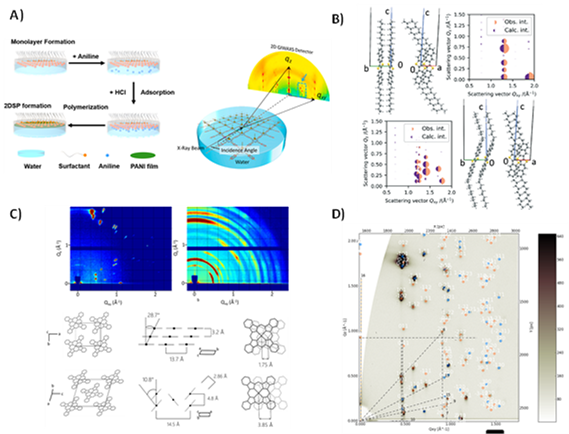
Figure 1 Examples of synchrotron X-ray scattering-based research in our group: A) in-situ synthesis and growth monitoring of layered organic 2D materials in a Langmuir trough. B) Advanced refinement calculations that reconstruct molecular packing from GIWAXS data. B-C) Monitoring and in-situ studies of polymorphism and polymorphic transitions. D) Unit cell reconstruction in multi-phase organic hetero-layer systems
As active users of hard and soft X-ray synchrotron beam lines, we study the morphological details of thin single crystals,[1] polycrystalline thin films of small molecules,[2–5] polymer thin films,[6,7] and organic 2D materials such as 2D polymers (like polyaniline)[8–10] or 2D metal-organic frameworks (MOFs).[11,12] In numerous works we successfully have used techniques such as grazing incidence wide/small-angle X-ray scattering (GIWAXS and GISAXS) to obtain unit cells, precise molecular geometry and molecular alignment relative to important device interfaces, data on defect densities, and potential polymorphism caused by temperature or fabrication conditions. One of our unique competences lies in the reconstruction of the precise molecular geometry in unit cells even based on the limited number of visible diffraction peaks one can obtain from thin film samples. We more and more emphasize the potential of performing such diffraction experiments in-situ, such as monitoring growth and polymerizing an organic 2D material on the water surface, tracing polymorphism in heating and cooling experiments,[2,4] and performing in-operando scattering at devices whose active layers are exposed to the beam.
- D. L. Gonzalez Arellano, E. K. Burnett, S. Demirci Uzun, J. A. Zakashansky, V. K. Champagne, M. George, S. C. B. Mannsfeld, A. L. Briseno, J. Am. Chem. Soc. 2018, 140, 8185.
- F. Talnack, S. Hutsch, M. Bretschneider, Y. Krupskaya, B. Büchner, M. Malfois, M. Hambsch, F. Ortmann, S. C. B. Mannsfeld, Mol. Syst. Des. Eng. 2022, 7, 507.
- K. Ortstein, S. Hutsch, M. Hambsch, K. Tvingstedt, B. Wegner, J. Benduhn, J. Kublitski, M. Schwarze, S. Schellhammer, F. Talnack, A. Vogt, P. Bäuerle, N. Koch, S. C. B. Mannsfeld, H. Kleemann, F. Ortmann, K. Leo, Nat. Mater. 2021, 20, 1407.
- Y. Diao, K. M. Lenn, W.-Y. Y. Lee, M. A. Blood-Forsythe, J. Xu, Y. Mao, Y. Kim, J. A. Reinspach, S. Park, A. Aspuru-Guzik, G. Xue, P. Clancy, Z. Bao, S. C. B. B. Mannsfeld, J. Am. Chem. Soc. 2014, 136, 17046.
- S. C. B. Mannsfeld, M. L. Tang, Z. Bao, Adv. Mater. 2011, 23, 127.
- M. Hambsch, T. Erdmann, A. R. Chew, S. Bernstorff, A. Salleo, A. Kiriy, B. Voit, S. C. B. Mannsfeld, J. Mater. Chem. C 2019, 7, 3665.
- X. Gu, J. Reinspach, B. J. Worfolk, Y. Diao, Y. Zhou, H. Yan, K. Gu, S. Mannsfeld, M. F. Toney, Z. Bao, ACS Appl. Mater. Interfaces 2016, 8, 1687.
- M. Ballabio, T. Zhang, C. Chen, P. Zhang, Z. Liao, M. Hambsch, S. C. B. Mannsfeld, E. Zschech, H. Sirringhaus, X. Feng, M. Bonn, R. Dong, E. Cánovas, Adv. Funct. Mater. 2021, 31, 1.
- T. Zhang, H. Qi, Z. Liao, Y. D. Horev, L. A. Panes-Ruiz, P. St. Petkov, Z. Zhang, R. Shivhare, P. Zhang, K. Liu, V. Bezugly, S. Liu, Z. Zheng, S. Mannsfeld, T. Heine, G. Cuniberti, H. Haick, E. Zschech, U. Kaiser, R. Dong, X. Feng, Nat. Commun. 2019, 10, 4225.
- K. Liu, H. Qi, R. Dong, R. Shivhare, M. Addicoat, T. Zhang, H. Sahabudeen, T. Heine, S. Mannsfeld, U. Kaiser, Z. Zheng, X. Feng, Nat. Chem. 2019, 11, 994.
- Z. Wang, L. S. Walter, M. Wang, P. S. Petkov, B. Liang, H. Qi, N. N. Nguyen, M. Hambsch, H. Zhong, M. Wang, S. Park, L. Renn, K. Watanabe, T. Taniguchi, S. C. B. Mannsfeld, T. Heine, U. Kaiser, S. Zhou, R. T. Weitz, X. Feng, R. Dong, J. Am. Chem. Soc. 2021, 143, 13624.
- M. Wang, Z. Zhang, H. Zhong, X. Huang, W. Li, M. Hambsch, P. Zhang, Z. Wang, P. St. Petkov, T. Heine, S. C. B. Mannsfeld, X. Feng, R. Dong, Angew. Chemie Int. Ed. 2021, 60, 18666.
.