


Path D - Biomolecular-Assembled Circuits
Compared to the other paths, a more unconventional approach is followed by the Biomolecular-Assembled Circuits Path (BAC). In our approach, complex biomolecular structures will serve as templates to achieve devices with a large variety of materials, functionalities and (1, 2 and 3-dimensional) geometrical arrangements which are not easily accessible by standard lithography techniques.
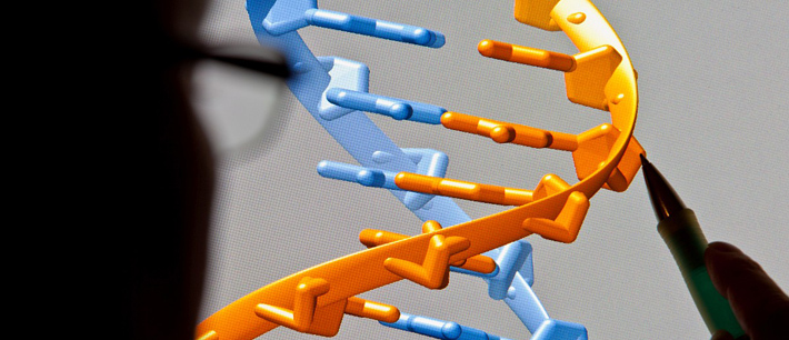
In particular, complex, three-dimensional DNA-based (deoxyribonucleic acid) scaffolds are used to create plasmonic, optoelectronic and electronic structures in a cost-effective and highly parallel manner. By integrating such components into established silicon-based electronics, functionalities and systems far beyond current boundaries will be enabled.
Path Leader: Prof. Andreas Fery
Path Co-Leader: Prof. Ralf Seidel
Path group leader: Dr. Thorsten-Lars Schmidt
BAC research groups:
- Prof. Dr. Stefan Diez
- Dr. Artur Erbe
- Prof. Dr. Alexander Eychmüller
- Prof. Dr. Andreas Fery
- Dr. Tobias König
- Prof. Dr. Rainer Jordan
- Prof. Dr. Michael Mertig
- Prof. Dr. Dirk Plettemeier
- Dr. Thorsten-Lars Schmidt
- Prof. Dr. Ralf Seidel
- Prof. Dr. Brigitte Voit
Most microelectronic components are fabricated by lithographic means. Despite the continuing miniaturization of components, there are a number of limitations to conventional lithography. For example, only few materials such as metals or certain semiconductors can be fabricated. Integrating more diverse functional materials such as plasmonically active metal or semiconducting nanoparticles, photonic crystals, or biomolecules is challenging. Next, only flat structures can be produced with lithography. Several layers can be stacked, but for example spherical nanoparticles or complex three-dimensional arrangements of components are difficult to produce. Finally, techniques such as electron-beam lithography or ion beam milling are sequential techniques and therefore expensive and not scalable.
Chemical synthesis on the other hand enables the cheap and scalable production of a large variety of functional nanomaterials including metallic and semiconducting nanoparticles, carbon nanotubes, silicon nanowires or (macro-) molecules.
To achieve functional devices, such materials need to be arranged and interconnected. For this, we are exploring the power of DNA (deoxyribonucleic acid) based self-assembly.
Our goal is to employ structural DNA nanotechnology for a massively parallelized low-cost fabrication of nanophotonic, optoelectronic and electronic devices for future electronics and communication. To achieve integrated devices and systems, larger complex and high-precision self-assembled structures may in the next step patterned with cheaper low-resolution lithographic techniques.
The BAC path covers 5 different topics areas:
Self-assembled plasmonic waveguides
Light will be guided through metallic nanoparticles arranged on DNA structures to demonstrate sub-wavelength optical short-range communication.
Plasmonic antennas
Top-down and bottom-up techniques will be combined to build optical antennas to enable coupling between near- and far-field effects.
DNA-templated heterostructures
Programmable/hierarchical self-assembly of nanostructures from different materials (e.g. polymers, metallic, semiconducting nanoparticles)
Modelling
Theoretical support for the design and optimization of optical devices.
Micro-nano interfacing
Most potential devices, require electrical and/or optical interfacing of the self-assembled nanostructures with the outside world to bridge the gap from nano to micro (to macro). For this, a selective and well-ordered deposition of the DNA-based structures is required.
The BAC path is working in close collaboration with the Carbon, Si-NW and HAEC paths.
June 22, 2016:
BAC reatreat in Lohmen.
May 2016:
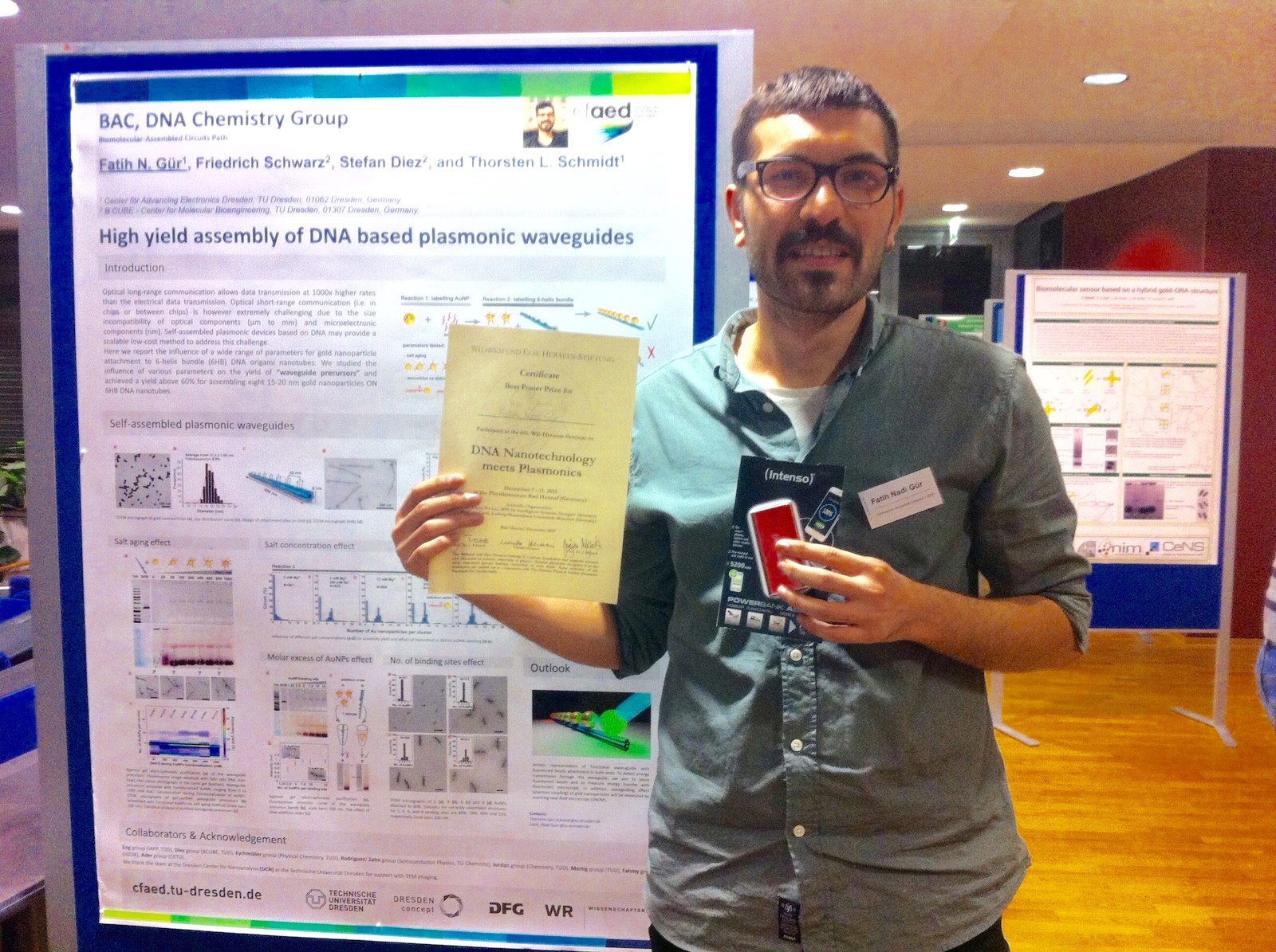
Paper by Gür et al. in ACS Nano: Toward Self-Assembled Plasmonic devices: High-Yield Arrangement of Gold Nanoparticles on DNA Origami Templates

February 2016:
Paper by Matthies et al in Nano Letters: Design and Synthesis of Triangulated DNA Origami Trusses

Dec. 11, 2015:
Fatih Gür (Schmidt lab) wins the poster prize at "DNA meets Plasmonics" in Bad Honnef for his poster "High yield assembly of DNA based plasmonic waveguides". Congratulations, Fatih!
Nov. 2015:
An enzymic oligonucleotide synthesis method developed at the Wyss Institute (Harvard) and the cfaed may radically decrease the price of oligonucleotides necessary to increase the complexity of DNA nanostructures or for applications in synthetic biology.
Read more: T. L. Schmidt et al. Nature Communications 2015.
Sept. 2015: BAC general assembly
cfaed Publications
Optimization of isopolar microtubule arrays
Reference
Rodney R Agayan, Robert Tucker, Takahiro Nitta, Felix Ruhnow, Wilhelm J Walter, Stefan Diez, Henry Hess, "Optimization of isopolar microtubule arrays", In Langmuir, ACS Publications, vol. 29, no. 7, pp. 2265–2272, 2013. [doi]
Bibtex
title={Optimization of isopolar microtubule arrays},
author={Agayan, Rodney R and Tucker, Robert and Nitta, Takahiro and Ruhnow, Felix and Walter, Wilhelm J and Diez, Stefan and Hess, Henry},
journal={Langmuir},
volume={29},
number={7},
pages={2265--2272},
year={2013},
publisher={ACS Publications},
doi={10.1021/la303792v}
}
Downloads
No Downloads available for this publication
Related Paths
Biomolecular-Assembled Circuits Path
Permalink
https://cfaed.tu-dresden.de/biomolecular-assembled-circuits?pubId=315