


Path A - Silicon Nanowire
The Silicon Nanowire Path (Silicon NW) follows the most “conventional” approach by virtue of using silicon. Nevertheless, the potential electronic properties of these nanowires go far beyond current silicon technologies. Besides very beneficial electronic properties, silicon nanowires can be configured to change transistors between p- and n-type dynamically. Potentially, complex functionality can thus be implemented with much smaller numbers of devices. In this context, the design of novel and fault tolerant computing algorithms that make use of the transistors’ multi-functionality is also targeted. Furthermore, silicon nanowires will be explored as a selective sensor platform for biomolecules, opening a completely new application domain.

Prof. Thomas Mikolajick
Path Leader: Prof. Thomas Mikolajick
Path Co-Leader: Prof. Gianaurelio Cuniberti
- Prof. Dr. Uwe Aßmann
- Prof. Dr. rer. nat. Johann W. Bartha
- Prof. Dr. Gianaurelio Cuniberti
- Prof. Dr. sc. techn. habil. Dipl. Betriebswissenschaften Frank Ellinger
- Prof. Dr. Alexander Eychmüller
- Prof. Dr. Christof Fetzer
- Prof. Dr. Sibylle Gemming
- Prof. Dr. Manfred Helm
- Prof. Dr. rer. nat. et Ing. habil. Michael Mertig
- Prof. Dr.-Ing. Thomas Mikolajick
- Dr. rer. nat. habil. Francesca Moresco
- Prof. Dr. rer. nat. habil. Oliver G. Schmidt
- Prof. Dr.-Ing. Michael Schröter
- Prof. Dr.-Ing. habil. Christian Georg Mayr
- Dr. Walter Weber (cfaed Research Group Leader - Nanowire Research Group)
- Prof. Dr. rer. nat. habil. Ehrenfried Zschech
Information processing systems with higher value than conventional ones are projected to emerge as possible successors of the current workhorse in electronics, the complementary metal–oxide–semiconductor (CMOS) technology. The Silicon Nanowire Path will focus on More-than-Moore and Beyond-Moore approaches, which exhibit functional reconfiguration by exploiting the unique combination of nanoelectronics with state-of-the-art Silicon (Si) technology.
Two different approaches, here called Tracks, will be followed to achieve reconfigurability at the Devices & Circuits Abstraction Layer. First, reprogrammable silicon nanowire (Si-NW) field effect transistors (FET) and fine-grain reconfigurable logic circuits and systems fabricated thereof will be studied. Second, reconfiguration of NW FETs by the attachment of bio-functional units will be investigated. The latter will enable building a novel multiplexer platform for complex bioelectrical transducer systems as required for the interaction between computing systems and biological components in strong interaction with the Biological Systems Path.
Both approaches are based on the same basic nanowire technology, are complementary, and can be combined with each other. At the system level, fault tolerant algorithms will be developed that make use of device reconfigurability during circuit operation. The results aim at providing sophisticated Beyond-Moore electronics with higher computational power and enhanced user interfacing capabilities by suggesting highly sensitive and highly specific bionanosensors.
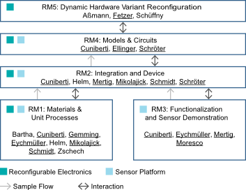 The work is organized into 5 thematic Research Modules (RMs) as illustrated in the table. Interweaving the RMs, two synergistic Tracks will be formed to tackle the objectives of the reprogrammable electronics and biosensor platform, respectively. The targeted objectives in the short term (2½ years) are to demonstrate a first generation of simple reconfigurable logic gates (NOR-NAND), a biosensor device example, first compact models, and algorithms that show the prospects of complete systems with these gates. To meet this schedule, available technologies and device data will be used at start. After 4 years, cascaded gate systems and oscillators with reconfigurable operation and different configurations will be provided. The corresponding system algorithms for dynamic reconfiguration upon failure will be developed. An optically configured Si-NW FET driven by semiconductor nanoparticles is to be shown. A multiplexed and selective transducer NW platform including integrated signal amplification will be demonstrated. The integration of biosensor devices in microfluidic systems and their testing under realistic conditions will pave the way towards nanosensor prototyping. Two new research group leader positions, Reconfigurable Nanowire Electronics and Nanowire Biosensor Devices, will be appointed for this Path that will lead the two Tracks.
23.07.
Flexible Future of Point-of-Care Disease Diagnostic
cfaed scientists at Leibniz Institute for Solid State and Materials Research Dresden (IFW), TU Dresden, and Nanoelectronic Materials Laboratory (NaMLab gGmbH) realized flexible light weight diagnostic platform enabling its cost efficient high-volume delivery to medical institutions worldwide.
The world-wide deployment of biomedical devices for health monitoring, point-of-care diagnostics and environmental sensing is hampered by their high cost that is not readily affordable for e.g. developing countries. The primary task is therefore to reduce the price of the devices and allow for their high-volume delivery in a cost efficient manner, e.g. container transportation. For the latter, a crucial aspect is to reduce the weight of the device.
Within the Silicon Nanowire Research Path (SiNW) of TU Dresden’s Cluster of Excellence ‘Center for Advancing Electronics Dresden’ (cfaed), the scientists realized a light weight and mechanically flexible diagnostic platform based on cost-effective highly sensitive Si nanowire field effect transistors fabricated on flexible polymeric foils, which are only 100 µm thick. The devices reveal a remarkable limit of detection for subtype H1N1 Avian Influenza Virus, which is considered as a global major risk for human health, exemplified by the declaration as pandemic to the 2009 swine-origin one. The devices on polymeric support are about 10 times lighter compared to their rigid counterparts realized on conventional Si wafers which make them cost efficient for high-volume delivery to medical institutions worldwide. The researchers envision that the realization of the sensitive diagnostic platform will allow the timely diagnosis of the viral or infectious diseases also in the developing countries.
This work was carried out at the Leibniz Institute for Solid State and Materials Research Dresden (IFW) in cooperation with the Chair of Materials Science and Nanotechnology of TU Dresden and NaMLab gGmbH.
The original work was published as a cover story of the recent issue of Advanced Healthcare Materials 10, 1517 (2015)
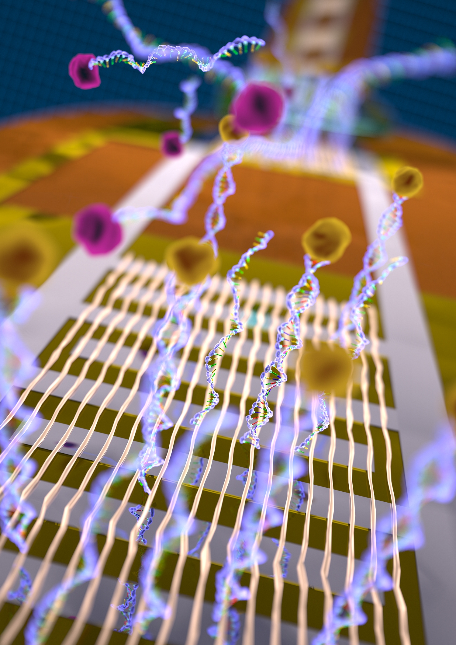
Image: Daniil Karnaushenko, IFW Dresden
cfaed Publications
Reconfigurable Si-Nanowire Field Effect Transistors as a Building Block for Post Moore Electronics
Reference
T. Mikolajick, A. Heinzig, J. Trommer, M. Grube, W. Weber, "Reconfigurable Si-Nanowire Field Effect Transistors as a Building Block for Post Moore Electronics".
Bibtex
title={Reconfigurable Si-Nanowire Field Effect Transistors as a Building Block for Post Moore Electronics},
author={Mikolajick, T and Heinzig, A and Trommer, J and Grube, M and Weber, W}
}
Downloads
No Downloads available for this publication
Related Paths
Permalink
https://cfaed.tu-dresden.de/silicon-nanowire?pubId=521